
Distance Measurement with Ultrasonic Sensors
Ultrasonics sensor has a crystal which can resonates with 40kHz signal. To drive the ultrasonic sensor, we should generate 40kHz square wave with 50% duty cycle. Fundamental logic behind measuring the distance with ultrasonic sensor using 40kHz PWM signal is phase shift between trigger and echo signals of transducers. Then, the phase shift will be up to 40 kHz at most. Let’s calculate the distance we can measure for the ultrasonic sensor triggered by a 40kHz continuous PWM signal.
The sound of speed in air is about 343 m/s. For 40kHz PWM signal, the period of it is 25 microseconds.
Generating PWM Signals
SG3525 – 40kHz PWM with 50% Duty Cycle
It is easy to see the distance is pretty low to measure distance or scan any part of room. So, we should modulate the 40kHz PWM signal with a specific frequency and a duty cycle. We can easily generate 40kHz PWM signal with SG3525 integrated circuit. Here is the circuit diagram:
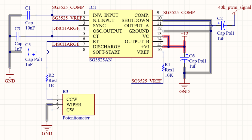
For more detail, you can read the datasheet of SG3525 from here.
To drive an ultrasonic sensor there is no need a dead-zone. So, R_D equal to zero. Then formula turns into:
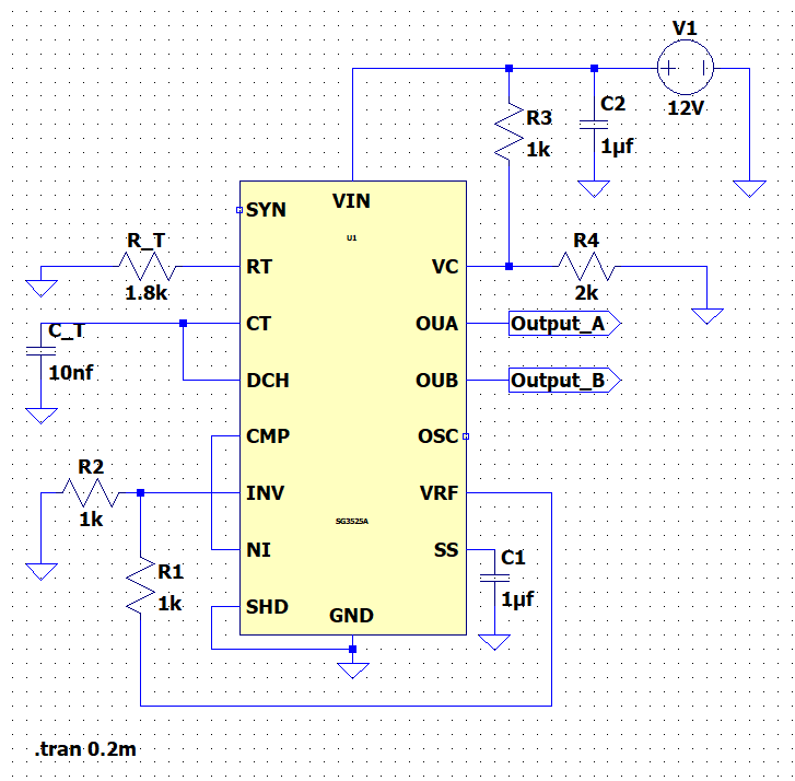
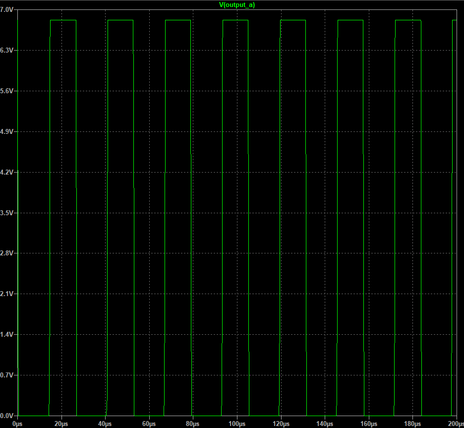
Key point of the SG3525 IC is frequency stands for frequency of oscillator. Therefore, if 40kHz PWM signal desired, calculations must be done with 80kHz oscillator frequency. For more detailed information you can examine the Block Diagram (p.2) on datasheet. We can analyse the SG3525 PWM circuit with Proteus, LTSpice or any other analysis software. Here is the simulation of LTSpice:
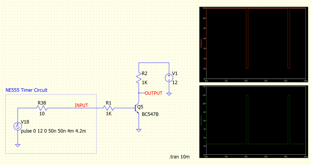
NE555 Timer – 240Hz PWM with 95% Duty Cycle
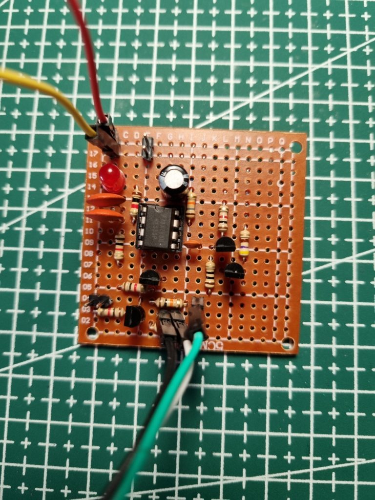
To trigger the ultrasonic transmitter, we should generate 40kHz PWM signal and generate 240Hz carrier square wave with 5% duty cycle. I built the circuit of 40kHz PWM signal above. Now, it is time to build 240kHz carrier square wave with 555 timer ic.
First of all, values of R1, R2 and C_t should be calculated. NE555 timer integrated circuit will be used in astable mode. The frequency formula is:
An excel sheet will be suit well to calculate those values quickly and repeatedly. Increase C to increase the period and reduce the frequency. Increase R1 to increase High Time (T1) without affecting the Low Time (T0). Increase R2 to increase High Time (T1), increase Low Time (T0) and decrease Duty Cycle.
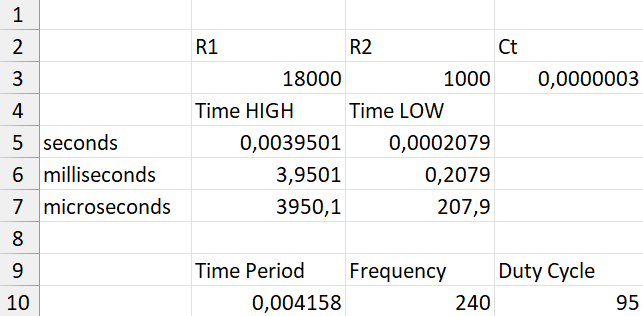
The values of R1, R2 and Ct are determined as shown Figure 4.
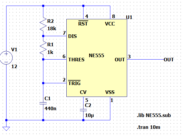
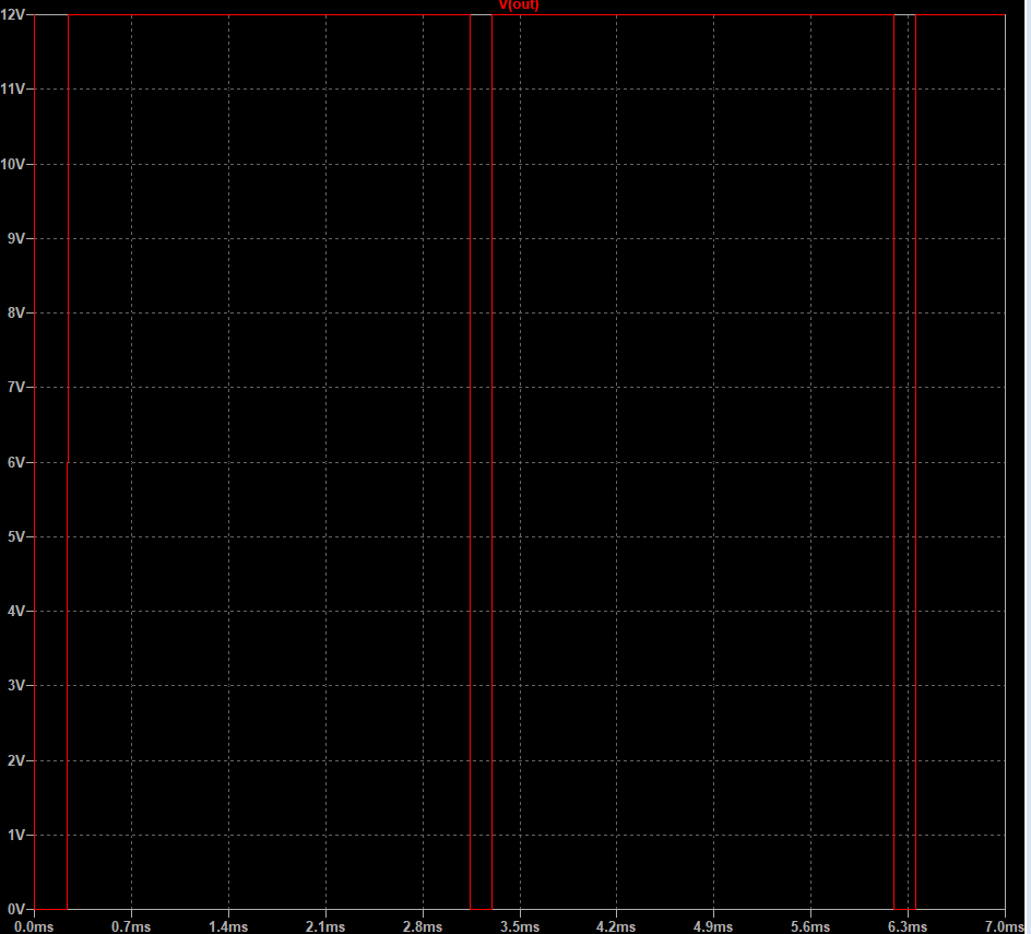
Let’s simulate the circuit that shown above and analyse the signal with a simulation tool. Here is the simulation schematic and results.
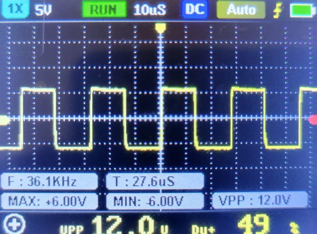
But there could be occur some problems in real life. Most common case is frequency could be disrupted from error rates of the resistor and the duty cycle could be disrupted from floating capacitance of breadboard. To analyse this kind of situations, after achieving successful results on simulation it is better to test the same circuit in real life. Here is the real-life experiment of SG3525 40kHz PWM with 50% duty cycle:

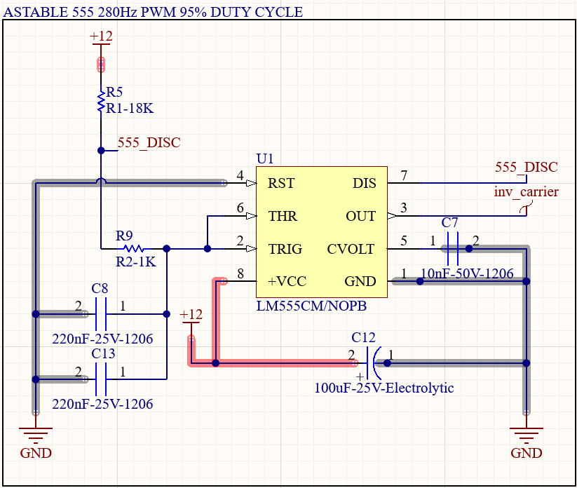
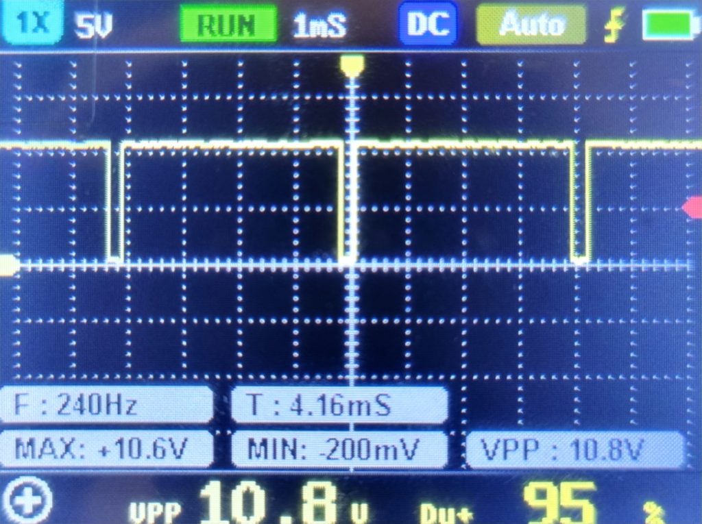
Let’s realize the circuit to generate 240Hz square wave with 95% duty cycle. Here is the real-life experiment and results:
Signal Inverter
Generate PWM with 95% duty cycle is easier than generating with 5% duty cycle. So, I preferred to generate the carrier signal with 95%. But we need to invert the signal. But how? Of course with using a BJT. Common-Emitter topology could be used as shown below:
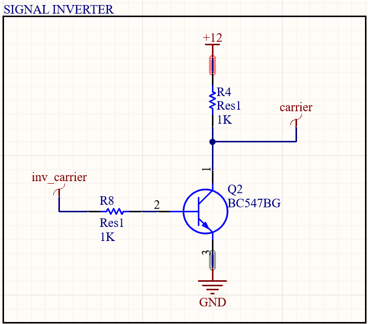
Common-Emitter topology offers:
- High current gain,
- Medium input resistance
- High output resistance.
Also, common-emitter topology inverts the output signal. Now, it is time to simulate.
Amplitude Modulation
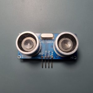
This circuit could be used but we will not use. I prefer to use emitter-follower topology for AM (Amplitude Modulation). I will not build the circuit that we need in this post. But I will examine the HC-SR04 module’s trigger pin as preliminary information.
With these three circuits, we get the carrier signal with 5% duty cycle. Now, it’s time to examine the HC-SR04 module to be ensure about we are on the right path.
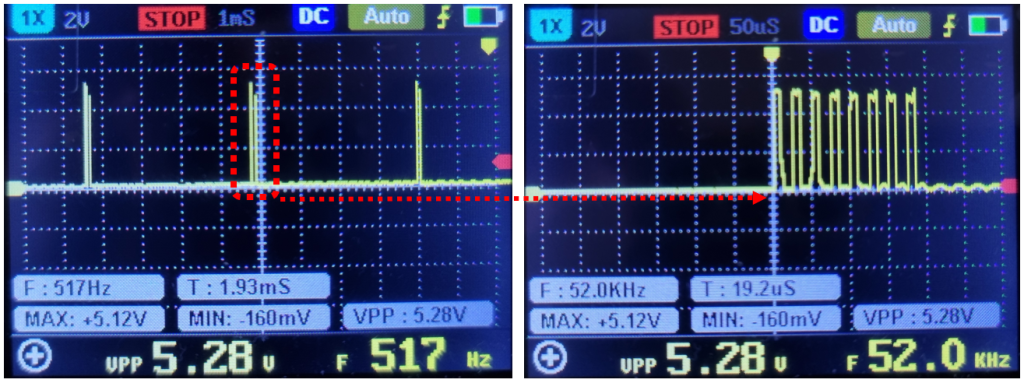
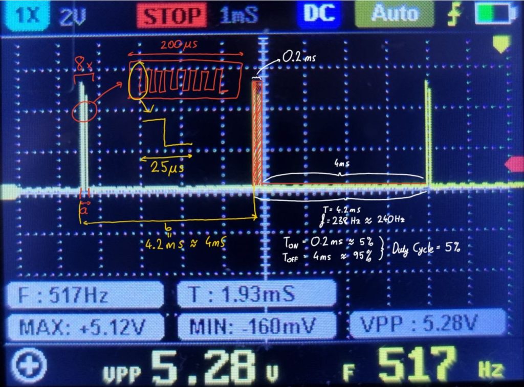
We can easily see the same thing from the images above. There are 8 40kHz PWM signals enveloped with 5% duty cycled 238 Hz carrier wave. In this position, we have 40kHz signal, 240Hz signal with 95% and 5% duty cycle. In a next post, I will examine the Amplitude Modulation to achieve desired results to drive an ultrasonic transmitter.
Leave a Reply